
Email format error
Email cannot be empty
Email already exists
6-20 characters(letters plus numbers only)
The password is inconsistent
Email format error
Email cannot be empty
Email does not exist
6-20 characters(letters plus numbers only)
The password is inconsistent

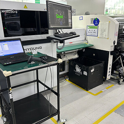
SPI (Solder Paste Inspection) refers to automated equipment designed to evaluate solder paste printing quality in Surface Mount Technology (SMT) production lines. As electronic components miniaturize (e.g., 01005 packages) and PCB densities increase, traditional visual inspections have become inadequate. Modern SPI systems employ 3D optical measurement technologies to achieve micron-level precision (±3μm) in detecting solder paste volume, height, and alignment deviations. Industry data from IPC standards indicates that 60-80% of SMT defects originate from solder paste printing errors, while SPI implementation increases defect interception rates to over 95%.
|
Aspect |
SPI |
AOI |
|
Inspection Stage |
Post-printing, pre-component placement |
Post-placement, pre/post-reflow |
|
Measurement Focus |
3D paste parameters (volume/height/offset) |
Component positioning/polarity |
|
Technology |
Structured light/Laser triangulation |
Multi-angle imaging |
|
Precision |
Micron-level (0.1-5μm) |
Sub-millimeter (0.05-0.1mm) |
|
Data Utilization |
Real-time printer adjustments |
Defect classification |
Synergy: SPI and AOI create a dual "prevention-verification" loop. SPI reduces pre-reflow defects by 70%, while AOI cuts final product failures by 50% (SMTA Industry Report).
SPI ensures uniform solder paste distribution within ±15% volume tolerance. For automotive ECU boards, the KOHYOUNG SPI machine detects 0.12mm³ volume deviations on 0.4mm² pads, preventing cold joints in critical signal pathways.
SPI's real-time feedback reduces printer calibration time from 30 minutes to 5 minutes. A telecom equipment manufacturer improved overall equipment effectiveness (OEE) from 82% to 93% after SPI implementation.
Compared to manual checks (2-3 sec/point, 15% missed defects), SPI achieves 0.5 sec/point inspection speeds with <1% error rates, supporting 100% production line coverage.
SPI-generated CPK (Process Capability Index) reports guide stencil design improvements. One manufacturer optimized aperture sizes using solder volume standard deviation (σ) data, increasing yields by 8%.
SPI employs structured light projection:
Case Study: A medical device manufacturer using the KOHYOUNG SPI machine reduced 0201 component paste volume variation from ±20% to ±8%, yielding 12% higher reliability.
|
Defect Type |
Detection Threshold |
Consequence |
|
Insufficient Paste |
<80% target volume |
Open circuits |
|
Excessive Paste |
>120% target volume |
Bridging |
|
Misalignment |
>25% pad width deviation |
Component skew |
|
Icicles |
>150% adjacent area height |
Electrical shorts |
|
Type |
Offline SPI |
Inline SPI |
|
Speed |
200-400 boards/hour |
600-1200 boards/hour |
|
Application |
Low-volume/high-mix |
High-volume production |
|
Precision |
±3μm |
±5μm |
|
Technology |
3D SPI |
2D SPI |
|
Principle |
Height measurement |
Grayscale analysis |
|
Precision |
±3μm (volume) |
±15μm (area) |
|
Cost |
High ($80,000+) |
Moderate ($30,000-$50,000) |
Market Forecast: The global SPI market will grow at a 9.2% CAGR from 2023 to 2028, expanding from $750 million to $1.21 billion (Source: MarketsandMarkets).