Email format error
Email cannot be empty
Email already exists
6-20 characters(letters plus numbers only)
The password is inconsistent
Email format error
Email cannot be empty
Email does not exist
6-20 characters(letters plus numbers only)
The password is inconsistent


Introduction
In modern electronics manufacturing, precision and quality are everything. Whether it is a smartphone, a medical device, or an industrial control unit. The smallest defect in a printed circuit board (PCB) can lead to failures, recalls, and financial losses. One crucial step ensures the reliability of PCB assembly. This step is solder paste inspection (SPI). As a solder paste inspection ODM, we understand the significance of this process. This process maintains the highest standards of quality. In this blog, we will explore why SPI is vital. We will also explain how it works. Finally, we will discuss how it benefits our business partners.
What Is Solder Paste Inspection?
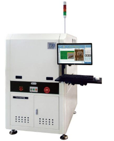
Solder paste inspection (SPI) is an advanced process. It is used to check the quality of solder paste deposits on a PCB. This inspection occurs before components are placed. The inspection ensures that the right amount of solder is applied. The solder must also be applied in the correct locations. This reduces the chances of defects. Examples of defects include bridging, insufficient solder, or misalignment.
Modern PCB components are microscopic in size. Even the slightest variation in solder paste volume can impact performance. This is why SPI has become a standard part of surface mount technology (SMT) assembly lines.
Why Solder Paste Inspection Matters
Preventing Defects Early
Detecting and correcting solder paste application issues is critical. This must happen before component placement. Early detection helps prevent costly rework. It also prevents potential product failures. If defects are discovered too late, fixing them becomes challenging. Late-stage fixes are also significantly more expensive.
Ensuring Consistent Quality
As a solder paste inspection ODM, we prioritize consistency and precision. SPI machines use high-resolution cameras. They also use laser-based scanning systems. These tools analyze solder paste deposits in detail. This ensures that every PCB meets high-quality standards. Consistency reduces variability in production.
Reducing Scrap and Rework Costs
Faulty solder paste application can lead to defects. These defects may not be easily repairable. By implementing SPI, manufacturers cut down on material waste. They also reduce time spent fixing errors. This ultimately saves money.
Improving Process Control
SPI provides valuable data. This data helps manufacturers fine-tune their stencil printing process. By analyzing trends, recurring issues can be identified. Manufacturers can then make adjustments. These adjustments improve efficiency. They also minimize defects.
How Does Solder Paste Inspection Work?
3D Imaging Technology
Most modern SPI machines use 3D measurement technology. This technology assesses solder paste volume, height, and shape. Traditional 2D inspection only captures surface-level data. In contrast, 3D imaging provides a more accurate representation.
Automated Optical Inspection (AOI)
Automated optical inspection systems use high-resolution cameras. They also use laser sensors. These tools capture images of the solder paste. The software compares these images against predefined standards. This detects inconsistencies.
Data Analysis and Reporting
SPI machines collect and analyze vast amounts of data. This happens in real-time. The information identifies trends. For example, some PCB areas may receive too much solder paste. Other areas may receive too little. This data-driven approach optimizes stencil printing. It also reduces defects over time.
Solder Paste Inspection in Our ODM Services
As a solder paste inspection ODM, we integrate SPI into our PCB assembly process. This ensures the highest quality for our customers. Our advanced SPI systems allow us to:
By choosing us as your ODM partner, you gain access to cutting-edge technology. You also gain expertise. This enhances the reliability of your electronic products.
The Future of Solder Paste Inspection
Electronic components continue to shrink. They are also becoming more complex. SPI technology is evolving to keep up. Emerging trends include:
AI and Machine Learning Integration
Artificial intelligence (AI) is being incorporated into SPI systems. This enhances defect detection accuracy. It also predicts potential issues before they occur.
Industry 4.0 and Smart Manufacturing
SPI plays a crucial role in smart factories. Here, interconnected machines adjust printing parameters automatically. Adjustments are based on real-time inspection data.
Higher Resolution and Faster Processing
Advancements in camera and sensor technology are occurring. These allow SPI machines to inspect PCBs with greater precision. They also enable faster inspections. This reduces production downtime.
Industry-Specific Demands
The stakes for flawless PCB assembly vary by industry. In medical devices, a solder defect could compromise life-saving equipment. Automotive electronics require zero defects. This is especially true for EVs and autonomous systems. Passenger safety depends on this. Aerospace applications demand extreme reliability. They must perform under harsh conditions. SPI acts as a safeguard. It aligns with stringent industry certifications. Examples include ISO 13485 for medical devices. Another example is IATF 16949 for automotive. This ensures compliance. It also reduces liability risks.
How SPI Works
Step-by-Step SPI Process

Challenges in SPI Implementation
Overcoming Common Hurdles
Case Study: SPI in Action
A consumer electronics manufacturer faced recurring failures. These failures occurred in smartphone PCBs. They were due to solder bridging. After implementing 3D SPI, defects dropped by 85% within three months. Real-time data revealed stencil misalignment. This happened during high-speed printing. Automated adjustments corrected the issue. This saved $500K annually in rework costs.
Future Trends: Deeper Dive
AI-Driven Defect Prediction
Machine learning models are trained on historical SPI data. They predict printer drift before defects occur. For example, AI might flag gradual stencil wear. This prompts preemptive replacement.
IoT-Enabled Smart Factories
SPI systems in Industry 4.0 ecosystems share data. They connect with ERP and MES platforms. This enables predictive maintenance. It also optimizes supply chains. Imagine SPI metrics triggering automatic solder paste reorders. This happens when usage trends exceed thresholds.
Best Practices for Effective SPI
ROI of SPI: By the Numbers
Custom SPI Solutions for ODMs
As an ODM, we tailor SPI systems to client needs:
Final Call to Action
Investing in SPI is not just about avoiding defects. It is about building a reputation for reliability. Partner with us to deploy SPI solutions. These solutions future-proof your production line. Contact our team today for a free audit. We will audit your SMT process. Let us transform your quality control. Transform it into a competitive advantage.